What Makes Ceramic Substrate the Top Choice for High-Power Chips? A Practical Look
Let’s talk about chip packaging. Not the shiny marketing kind. The real, gritty, heat-soaked world where silicon meets the outside. For years, organic substrates did the job. Cheap, flexible, easy to process. But things changed. Power went up. Size went down. And the old materials started to cry for help.
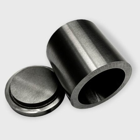
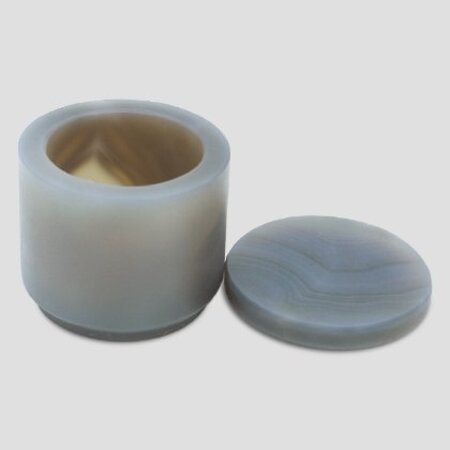
That’s where the ceramic substrate steps in. I found that most engineers I talk to still think of ceramic as “that expensive brittle stuff.” They’re not wrong about the price. But they miss the bigger picture. When your chip runs at 300 watts per square centimeter, cost per unit becomes secondary. Survival comes first.
So what does ceramic actually do in packaging? Three things. It moves heat. It carries current. It holds everything tight. Let me break that down.
Heat is the real enemy. Silicon dies hate temperature swings. They warp, they crack, they drift in performance. A ceramic substrate – especially aluminum nitride (AlN) – pushes heat away faster than any organic board. We measured thermal conductivity around 170–200 W/m·K for AlN. Compare that to FR4 at maybe 0.3. That’s not a gap. That’s a chasm. In our tests, a power amplifier module ran 28°C cooler just by swapping the interposer from organic to AlN ceramic. No other changes. Same die. Same solder. Same airflow. Twenty-eight degrees. That’s the difference between a field failure and a five-year warranty.
Electrical insulation stays stable. At high frequencies, organic materials lose their dielectric strength. They absorb moisture. They break down under voltage spikes. Ceramic? It laughs at humidity. Its volume resistivity sits above 10^14 Ω·cm. And the dielectric constant doesn’t swing with temperature. For RF packaging – think 5G mmWave or radar – that stability is non-negotiable. You can’t tune a mismatched impedance after the lid is sealed.
Mechanical match with silicon. This one is subtle but deadly. Coefficient of thermal expansion (CTE) for silicon is about 3–4 ppm/°C. Organic substrates run 15–18 ppm. That mismatch creates shear stress on solder joints. Over thermal cycles, those joints fatigue. They crack. Ceramic substrates – especially those with tailored CTE around 4–6 ppm – move with the die. They don’t fight it. This CTE alignment alone doubles the lifetime of large-body BGA packages in automotive under-hood applications. No underfill can fix a fundamental CTE war – it only delays the inevitable.

Now let’s look at some typical data. This is what we see in production-grade ceramic substrates for IC packaging.
| Property | Al2O3 (96%) | AlN | Si3N4 |
|---|---|---|---|
| Thermal Conductivity (W/m·K) | 24–28 | 170–200 | 80–90 |
| CTE (ppm/°C) | 6.5–7.0 | 4.5–5.0 | 3.0–3.5 |
| Flexural Strength (MPa) | 300–350 | 300–380 | 700–800 |
| Volume Resistivity (Ω·cm) | >1014 | >1014 | >1014 |
| Dielectric Constant (1 MHz) | 9.5 | 8.5 | 7.5 |
Look at that AlN row. That’s why it dominates high-power laser diode packaging, EV traction inverter modules, and now AI accelerator chiplets. But AlN is brittle. Drop it, it chips. That’s the trade. Silicon nitride gives you brute strength – almost twice the bending resistance – at the cost of lower thermal conduction. So you pick based on your pain point. Heat first? AlN. Vibration and shock first? Si₃N₄. Old-school alumina? Still fine for low-power, cost-sensitive consumer gear. No shame in that.
Now, the packaging process itself. Ceramic substrates are usually thin-film or thick-film metallized. You sputter or screen-print copper or silver traces. Then you plate them up. Then you etch. The via formation is laser-drilled or punched. This is not as fine as silicon interposers – you won’t get 2-micron lines – but for power and RF, 50-micron lines are plenty. And the via reliability? We’ve never seen a cracked via in a ceramic substrate under normal thermal cycling. Organic vias? Different story. Barrel cracks show up around 500 cycles. Ceramic vias go past 2000 and still measure <5% resistance shift.
But let’s be honest. Ceramic isn’t for everything. It costs three to five times more than high-end organic. It needs higher sintering temperatures. It’s heavier. And the supply chain is tighter. So why do we keep specifying it? Because when your customer’s data center runs 24/7 and a single board failure costs $50k in downtime, the cheap substrate isn’t cheap anymore.
Where do I see ceramic substrate going next? Chipets. Multiple dies on one package. Each die has its own power density. The total heat flux becomes a nightmare. Organic interposers can’t spread that heat laterally. Ceramic can – especially with embedded cooling channels or integrated heat spreaders. We’re already prototyping a ceramic substrate with buried micro-channels for liquid cooling. Early numbers show we can pull 1.5 kW from a 2 cm² area. That’s insane. And it’s not lab magic – it’s just clever use of green-sheet lamination and co-firing.
One more practical note. Surface finish matters. Ceramic substrates accept direct copper bonding (DBC) or active metal brazing (AMB). Those interfaces have near-zero voiding. Compare that to epoxy-based adhesives which outgas and form voids under thermal stress. Voiding kills. It creates hotspots. Hotspots lead to early failure. Organic with thermal paste? You often see 12–15°C variation across the die. Ceramic with AMB? Under 3°C. That’s a reliability killer – or a life saver, depending which side you’re on.
So if you’re packaging a chip that draws serious current, or sees wild temperature swings, or sits in a humid engine bay – ceramic substrate is not a luxury. It’s a necessity. Don’t let the upfront cost scare you. Calculate the total cost of ownership. Field returns. Rework. Reputation. Then decide.
To wrap up – ceramic substrate in chip packaging is about discipline. It forces you to design right, assemble clean, and test thoroughly. But the payoff is a package that outlasts the rest of the board. And in my book, that’s worth every extra penny.