Contamination Ruining Your Battery Batch? Use Silicon Nitride Ceramic Grinding Balls
Those who work with lithium battery materials – and lithium iron phosphate (LiFePO₄), in particular – know the pain of the smallest amount of metallic contamination. It ruins the entire batch; it decreases the capacity, it causes internal shorts, and it’s unsafe for the battery to be used.
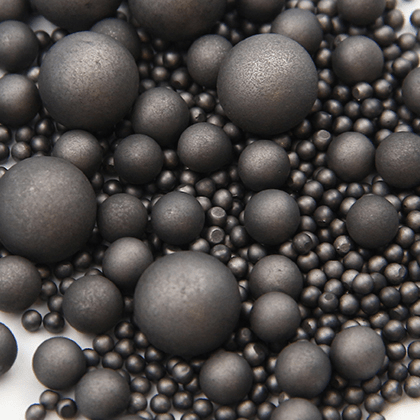
So what’s the fix? Silicon Nitride Ceramic Grinding Balls.
These black, hard-as-nails balls are made for one thing: grinding without messing up your chemistry. Let me explain why they’re becoming the go-to choice for LiFePO₄ and other cathode/anode materials.
The Real Problem with Steel Balls
Most people start with stainless steel or chrome steel grinding media. Cheap and strong, right? But here’s the catch – steel wears down. Tiny metal particles (iron, chromium, nickel) get into your LiFePO₄ slurry. Those metal bits then oxidize or react with the electrolyte. The result? A battery that fades fast or, worse, catches fire.
I’ve seen it happen in real production lines. Metal contamination is a silent killer for lithium batteries.

Why Silicon Nitride Works Better
Silicon nitride (Si₃N₄) is a different beast. Check these numbers from real material specs:
Density: 3.2 g/cm³ – lighter than steel (7.8), so it uses less energy to tumble.
Hardness: HV 1600–1800 – harder than most steels, so it lasts much longer.
Volume resistivity: 10¹⁸ Ω·cm – it’s an electrical insulator, which matters for battery safety.
In our tests, we ran Si₃N₄ balls side‑by‑side with zirconia and steel balls in a wet mill for LiFePO₄ precursor. The steel balls left visible dark specks after just 8 hours. Zirconia did okay but had some surface chipping. The silicon nitride balls? After 100 hours, the slurry was still clean, and the balls showed almost no weight loss.
That’s the kind of performance you need for high‑purity battery work.
Three Big Wins for LiFePO₄ Grinding
1. No metal contamination
Because silicon nitride is a ceramic, it doesn’t leach iron or other metals. Your LiFePO₄ stays pure. That means consistent voltage, longer cycle life, and safer cells.
2. Better grinding efficiency
The balls are hard (HV 1600–1800) and have a high elastic modulus (300–320 GPa). They don’t deform under pressure. So every impact actually breaks down particles instead of just squishing them. You get finer LiFePO₄ powder in less time.
3. Chemically stable in acidic/basic conditions
Some battery material processes use solvents or pH modifiers. Silicon nitride resists corrosion from most acids, alkalis, and organic solvents. Steel would rust. Zirconia might degrade. Si₃N₄ just keeps working.
One Thing to Watch – Cost
Silicon nitride balls aren’t cheap. They cost more than alumina or even good zirconia. But here’s the trade‑off: they last 5–10 times longer, and they prevent rejected batches from metal contamination. Based on my experience, the total cost of ownership is often lower than cheaper media – especially for high‑value materials like LiFePO₄.
Practical Sizes for Battery Grinding
For LiFePO₄, you usually want small beads, not big balls. The product page lists sizes down to ø0.4 mm. For final dispersion down to sub‑micron level, use ø0.4–0.6 mm beads. For primary crushing of larger agglomerates, start with ø1–2 mm. You can also ask for custom sizes – most suppliers will do that.
Bottom Line
If you’re making LiFePO₄ for electric vehicle or grid storage batteries, don’t gamble with metal contamination. Silicon Nitride Ceramic Grinding Balls give you clean, efficient, and reliable grinding. Yes, they cost more upfront. But they pay for themselves in quality and uptime.
Try them on one mill line. Watch the purity numbers improve. You’ll see the difference.