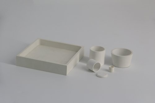
In the equally mindful and intensive field of semiconductor manufacturing, where even the smallest flaw can completely ruin production runs, and an entire production line requires absolute flawless execution, precision boron nitride crucibles have become vital in recent years. They are simply best suited for the production of ultra-pure silicon and compound semiconductor electronics.
What Makes Slicing and Dicing So Demanding
Both Cz and Kyropoulos techniques sapphire methods of semiconductor crystal growing which involves melting raw materials developing into very high temperatures (sometimes 1400-2100 °C).The crucible containing this molten material faces brutal challenges:
Intense Heat & Thermal Shock: Rapid heating and cooling cycles are common.
Purity is Paramount: Any contamination leached from the crucible walls directly degrades crystal quality and device performance.
Chemical Reactivity: Molten silicon and many compound semiconductors (GaAs, InP, GaN) aggressively react with most container materials.
Wetting Issues: Sticking between the crystal melt and crucible wall causes stress and defects during growth or removal.
How Boron Nitride Crucibles Solve Semiconductor Challenges
This is where the exceptional properties of hexagonal Boron Nitride shine:
Unmatched Chemical Inertness: BN crucibles exhibit extraordinary resistance to reaction with molten silicon, gallium arsenide (GaAs), indium phosphide (InP), gallium nitride (GaN), and aluminum oxide (Al₂O₃ – sapphire). They prevent crucible-derived contamination (like oxygen from quartz or carbon from graphite) that ruins crystal integrity.
Superior Thermal Shock Resistance: Unlike brittle ceramics, Crucibles can withstand the rapid temperature swings inherent in crystal pulling or cooling without cracking – essential for process reliability and crucible longevity.
Dewetting Surface: Boron nitride of high quality does not melt and semiconductors do not adhere to it. This provides better separation of crystals, allows simpler cleaning in the post-cleaning phase, and reduces the stresses induced defects in the growing crystal.
High Thermal Conductivity: The ability of BN to conduct heat is to facilitate better temperature uniformity within the melt which is done to assist in maintaining smoother and more consistent growing crystals.
High Temperature Stability: These crucibles retain their structure and efficiency after the high temperatures of melting the semiconductor materials into liquid form, in an inert or vacuum atmosphere.
High Purity: The state of the art processes enable the manufacture of Boron Nitride Crucibles with impurities in extremely low concentrations or even parts per million (ppm), ensuring the purity of the melt.
Key Semiconductor Applications for BN Crucibles
Monocrystalline Silicon (Czochralski Method): While large Cz pullers often use fused quartz crucibles, BN Crucibles are frequently employed as:
Protective Coatings/Liners: A layer of BN applied inside the quartz crucible acts as a barrier. It drastically reduces oxygen dissolution into the silicon melt (improving yield and quality) and prevents silicon melt adhesion to quartz, extending the quartz crucible’s life.
Crucibles for Specialized Silicon: For certain high-purity or specialized silicon applications, pure BN crucibles are used directly.
Compound Semiconductor Crystal Growth (GaAs, InP, GaN): Growing crystals like Gallium Arsenide (GaAs) for lasers and LEDs, Indium Phosphide (InP) for photonics, or Gallium Nitride (GaN) for power electronics demands BN crucibles. Their inertness prevents reaction with volatile group V elements (As, P) and contamination from the crucible itself is unacceptable for these sensitive materials.
Sapphire (Al₂O₃) Crystal Growth (Kyropoulos Method): Boron Nitride is the standard crucible material for melting aluminum oxide to grow large sapphire crystals used as substrates for LEDs, optical windows, and watch covers. Its non-wetting property is crucial for releasing the massive sapphire boule.
Advantages Over Traditional Crucible Materials
vs. Quartz: BN has vastly superior thermal shock resistance, higher maximum use temperature (inert/vacuum), and prevents silicon-oxygen contamination. Quartz softens and reacts.
vs. Graphite: BN is chemically inert to molten semiconductors (doesn’t form carbides), electrically insulating, and doesn’t introduce carbon contamination – a critical failure point for many semiconductors. Graphite reacts readily.
vs. Alumina (Al₂O₃): BN has far better thermal shock resistance and is non-wetting. Alumina can contaminate melts with aluminum ions and often bonds strongly to the crystal.
Boron Nitride Crucibles serve more than the purpose of containing something; their usefulness is a vital part of the process in the semiconductor industry. Their remarkable mixture of extreme thermal stability, ultra-high purity, non-wetting attributes, and chemical inertness leads to higher yields, lower rates of defects, and superior quality of crystals in the production of compound semiconductors, silicon wafers, and sapphire substrates. As newer materials are incorporated and the power demand becomes higher, smaller features and unparalleled performances for semiconductor devices leads to the growing need for Boron Nitride high-performance crucibles.