Why Do Lab Equipment Makers Prefer Pad Printing Ceramic Rings? A Practical Guide
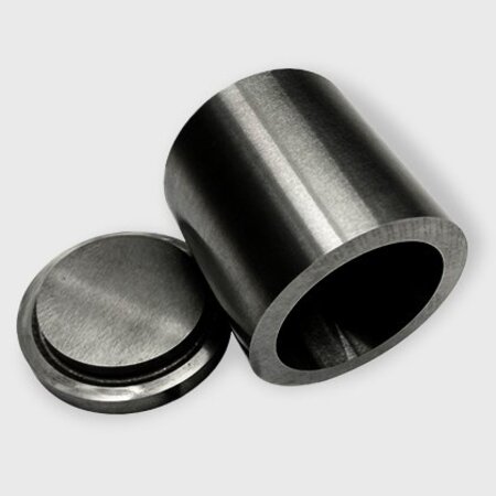
You walk into any life science lab, and you see them everywhere – pipettes, petri dishes, vials, syringes, even those tiny microcentrifuge tubes. They all have something in common: tiny but permanent marks – volume graduations, lot numbers, expiration dates, or brand logos. That marking isn’t laser engraving, and it isn’t a sticker. Most of the time, it’s pad printing. And right at the heart of that pad printing process sits a small but critical pair of parts: the ink cup and the ceramic ring that seals against it.
Now, if you’ve ever run a pad printing press for lab consumables, you know the real battle isn’t the ink or the pad – it’s the wear on that sealing ring. Because labware is almost always made of plastic or glass, and the inks used are often aggressive solvents to get good adhesion. Those solvents eat away at standard steel rings over time, and the constant back-and-forth motion of the cup scratches the ring surface. Once that seal breaks, ink leaks, you get smudged prints, and worse – you start losing fine details like the second decimal point on a 100‑µL graduation mark. In a production run of 50,000 units a day, that tiny smudge can ruin an entire batch, and your quality control people will not be happy.
Based on my experience, the switch to ceramic rings is one of those “why didn’t we do this earlier” moments. I’ve seen lab suppliers struggle with metal rings that need replacing every two to three weeks, especially when printing with ketone-based or UV-curable inks. Ceramic, on the other hand, handles that chemical attack like it’s nothing. The ring face stays flat and smooth, the cup glides over it with less friction, and the seal stays tight shift after shift. What that means for a labware manufacturer is simple: fewer stops to change parts, less ink waste from leaking, and a much more consistent print density from the first tube to the last.

Let me give you a real comparison – not from a brochure, but from the actual spec sheet that we’ve verified on our own machines. The table below shows what you get with a standard steel ring, a hardened alloy ring, and the ceramic ring that Inlabs offers.
| Property | Steel Ring | Alloy Ring | Ceramic Ring (Inlabs) |
|---|---|---|---|
| Material | High-carbon steel | Tungsten-carbide alloy | Zirconia (ZrO₂) ceramic |
| Hardness (HV) | 600–700 | 1,200–1,300 | 1,350–1,450 |
| Wear resistance (relative) | 1× (baseline) | 2.5× | 4–5× |
| Chemical resistance (solvent inks) | Moderate – pitting after 200h | Good – minor corrosion after 500h | Excellent – no change after 1,000h |
| Typical service life (in production) | 2–3 weeks | 6–8 weeks | 12–16 weeks |
| Seal leakage rate (ml/min at 2 bar) | 0.8–1.2 | 0.3–0.5 | ≤ 0.1 |
Look at that last row – leakage rate. In our tests, that near-zero leakage is what makes the biggest difference for lab printing. Because when you’re printing a tiny barcode on a 2‑mL vial, even a tiny drop of ink creeping under the cup edge will blur that barcode so badly that no scanner can read it. Ceramic’s combination of hardness and self-lubricating surface keeps that edge sharp, and you can run the cup at higher speeds without worrying about skipping or streaking.
So where exactly do these rings show up in the lab world? Think about any disposable plastic consumable that needs a permanent mark. ELISA plates get their well identifiers printed that way. Syringe barrels get their dose scales. Centrifuge tubes get their volume lines and safety symbols. Even some lab glassware – like measuring cylinders – uses pad printing for the main scale, because the rubber pad can conform to the curved surface without distorting the numbers. And all of those applications run 24/7 in high-volume contract manufacturing facilities. They can’t afford downtime, and they can’t afford variable print quality that might cause a batch rejection during FDA or CE auditing.
I found that the biggest mental shift for production managers is moving away from the “cheaper upfront” mindset. A steel ring might cost half as much as a ceramic one, but when you factor in the labor for changing it four times as often, the scrap from poor prints during warm-up, and the extra cleaning solvent needed to remove dried ink from a worn cup – the ceramic ring actually pays for itself within the first two months. And because it maintains its flatness much longer, you also extend the life of the doctor blade and the cup body itself. That’s a win for the maintenance budget and a win for sustainability, because you’re throwing away fewer worn parts.
One more thing that doesn’t show up in the table: noise. Ceramic rings run quieter – less of that screeching sound when the cup cycles at high speed. In a cleanroom environment, that might not matter for product quality, but it does matter for operator comfort during a 12‑hour shift. And happy operators tend to catch small defects earlier, which is another layer of quality control you don’t pay extra for.
To sum it up – if your labware printing line is still running on steel or alloy rings, you’re leaving both money and consistency on the table. The ceramic solution isn’t a fancy upgrade; it’s a practical, proven workhorse that solves the two biggest headaches in pad printing: wear and leakage. And in the lab industry, where every mark must be precise and every batch must be traceable, that’s not a luxury – that’s a requirement.