Pyrolytic Boron Nitride Crucible for Semiconductors: What Makes It the Top Choice?
Let‘s talk about making the stuff inside your phone. Not the screen, but the chips that make it fast. Those chips often start life as a single crystal of something like Gallium Arsenide, or GaAs. Growing that crystal? It’s tricky. You‘re dealing with insane temperatures, materials that don’t want to behave, and you need the final result to be absolutely pure. One speck of contamination and the whole thing is scrap.
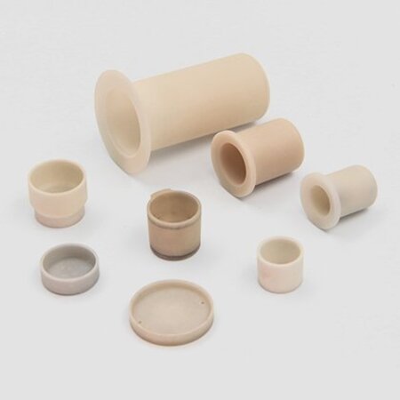
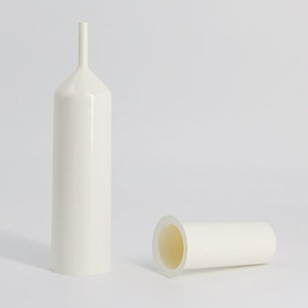
So, what do you hold this molten, temperamental material in? For decades, the answer has been the same: a Pyrolytic Boron Nitride Crucible, or PBN crucible.
Why this specific material? It comes down to three things: purity, thermal behavior, and a refusal to react with anything.
First, the purity angle.
These crucibles aren‘t machined from a block. They’re built in a furnace, atom by atom, through a process called chemical vapor deposition. Think of it like growing a ceramic crystal directly onto a mold. Because of how it‘s made, there’s no binder, no impurities sneaking in from a pressing tool. It‘s just boron and nitrogen, in a very ordered structure.
In our tests, switching to a high-quality PBN crucible often cleaned up the background impurities in the crystal immediately. You see it right there in the secondary ion mass spectrometry data.
Second, the heat.
This is the clever part. PBN has what we call anisotropic thermal conductivity. That’s a fancy way of saying it conducts heat very well in one direction (along the surface, the “a” direction), but acts as an insulator in the other (through the wall, the “c” direction). For crystal growth, this is gold. It means the heat spreads out evenly across the melt, avoiding cold spots. But it doesn‘t let heat leak straight out the sides. This uniform temperature profile is critical for growing a single crystal, not a mess of polycrystals.
Third, it’s chemically inert.
Molten Gallium and Arsenic are aggressive. They want to stick to things, react with things. Standard ceramics would get eaten alive, and those impurities would end up in your crystal. PBN doesn‘t play that game. It doesn’t wet easily, and it doesn‘t react. So after the growth run, the crucible often cleans up nicely and can be used again. That’s not always possible with other materials.
You‘ll find these crucibles in two main spots. One is in MBE (Molecular Beam Epitaxy) machines, where they hold the source materials that get evaporated into thin beams. The other is in bulk crystal growth furnaces, using techniques like the Liquid Encapsulated Czochralski method.
So, when you see a high-performance semiconductor, remember the humble container it was born in. The Pyrolytic Boron Nitride Crucible doesn’t just hold the melt. It shields it. It shapes the heat. It lets the crystal grow the way it should.